
-
Products
-
Featured Products
-
IT infrastructure
- Hard Drives
- OEM Souring
- CPU
- IT infrastructure Memory
- Spare Parts
- Cables
- Power Supply Units
- Adapters
- Controllers
- Server
- Switch
- Network Cards
- IT infrastructure Accessories
- Storage Machines
- Systemboard
- Sfp
- Harddrives
- Heatsink
- Fan
- Rack Options
- Licenses
- Battery
- IT Racks
- Graphics
- Io Expansions
- Routers
- San
- Access Point
- Blades
- Firewalls
- Expansion Cards
- Software
- Chassis
- Flex System
- Ups
- Wifi Controller
- Bladecenters
- Rack Mounts
- Monitors
- Antenna
- Phones
- Hmc
- Hard To Find
- END - OF - LIFE
- Electronic Wholesale
- 88E series
- Maxim Series
- TPS series
- STM series
- HOT - SALES and EOL Components
- SEE ALL

-
IT infrastructure
-
Integrated Circuits (ICs)
- Integrated Circuits (ICs) Kits
- Clock/Timing
- Data Acquisition
-
Embedded
- Embedded - CPLDs (Complex Programmable Logic Devices)
- Embedded - DSP (Digital Signal Processors)
- Embedded - FPGAs (Field Programmable Gate Array)
- Embedded - Microcontrollers
- Embedded - Microcontrollers - Application Specific
- Embedded - Microprocessors
- Embedded - PLDs (Programmable Logic Device)
- Embedded - System On Chip (SoC)
- SEE ALL
-
Interface
- Interface - Analog Switches - Special Purpose
- Interface - Analog Switches, Multiplexers, Demultiplexers
- Interface - CODECs
- Interface - Controllers
- Interface - Drivers, Receivers, Transceivers
- Interface - Encoders, Decoders, Converters
- Interface - Filters - Active
- Interface - I/O Expanders
- Interface - Modems - ICs and Modules
- Interface - Sensor and Detector Interfaces
- Interface - Serializers, Deserializers
- Interface - Signal Buffers, Repeaters, Splitters
- Interface - Signal Terminators
- Interface - Specialized
- Interface - Telecom
- Interface - UARTs (Universal Asynchronous Receiver Transmitter)
- Interface - Voice Record and Playback
- Interface - Sensor, Capacitive Touch
- SEE ALL
- Linear
-
Logic
- Logic - Gates and Inverters - Multi - Function, Configurable
- Logic - Buffers, Drivers, Receivers, Transceivers
- Logic - Comparators
- Logic - Counters, Dividers
- Logic - FIFOs Memory
- Logic - Flip Flops
- Logic - Gates and Inverters
- Logic - Latches
- Logic - Multivibrators
- Logic - Parity Generators and Checkers
- Logic - Shift Registers
- Logic - Signal Switches, Multiplexers, Decoders
- Logic - Specialty Logic
- Logic - Translators, Level Shifters
- Logic - Universal Bus Functions
-
PMIC
- PMIC - Power Over Ethernet (PoE) Controllers
- PMIC - Power Supply Controllers, Monitors
- PMIC - RMS to DC Converters
- PMIC - Supervisors
- PMIC - Thermal Management
- PMIC - V/F and F/V Converters
- PMIC - Voltage Reference
- PMIC - Voltage Regulators - DC DC Switching Controllers
- PMIC - Voltage Regulators - DC DC Switching Regulators
- PMIC - Voltage Regulators - Linear
- PMIC - Voltage Regulators - Linear Regulator Controllers
- PMIC - Voltage Regulators - Linear + Switching
- PMIC - Voltage Regulators - Special Purpose
- PMIC - AC DC Converters, Offline Switchers
- PMIC - Battery Chargers
- PMIC - Battery Management
- PMIC - Current Regulation/Management
- PMIC - Display Drivers
- PMIC - Energy Metering
- PMIC - Full, Half - Bridge Drivers
- PMIC - Gate Drivers
- PMIC - Hot Swap Controllers
- PMIC - Laser Drivers
- PMIC - LED Drivers
- PMIC - Lighting, Ballast Controllers
- PMIC - Motor Drivers, Controllers
- PMIC - OR Controllers, Ideal Diodes
- PMIC - PFC (Power Factor Correction)
- PMIC - Power Distribution Switches, Load Drivers
- PMIC - Power Management - Specialized
- PMIC - Voltage Regulators - Linear, Low Drop Out (LDO) Regulators
- SEE ALL
- Specialized ICs
- Memory
- Audio Special Purpose
- SEE ALL
-
Discrete Semiconductor Products
- Current Regulation - Diodes, Transistors
- IGBTs - Arrays
- Thyristors—SCRs
-
TRANSISTORS
- Transistors – FETs, MOSFETs – Single
- Transistors - FETs, MOSFETs Arrays
- RF Transistors (BJT)
- Transistors - FETs, MOSFETs - RF
- Transistors - Special Purpose
- Transistors (BJT) - Arrays
- Transistors (BJT) - Arrays, Pre - Biased
- Transistors (BJT) - Single
- Transistors (BJT) - Single, Pre - Biased
- Darlington Transistor
- SEE ALL
- Bridge Rectifiers
- Diacs, Sidacs
- Diodes - Zener - Arrays
- Diodes - Zener - Single
- Diodes, Rectifiers - Arrays
- Diodes, Rectifiers - Single
- FETs - Arrays
- FETs - Single
- IGBTs - Modules
- IGBTs - Single
- JFETs (Junction Field Effect)
- Power Drivers - Modules
- RFFETs
- SCRs - Single - Modules
- SCRs - Single
- Triacs
- Variable Capacitance Diodes (Varicaps, Varactors)
- RF Diodes
- SEE ALL
- Memory Cards, Modules
-
Sensors, Transducers
- Sensor Interface Junction Blocks
- Sensors, Transducers -Magnets Sensor -Matched Magnets
- Sensors, Transducers -Position Sensors- Angle, Linear Position Measuring
- Sensor Cable Assemblies
-
Optical Sensors
- Optical Sensors - Ambient Light, IR, UV Sensors
- Optical Sensors - Photo Detectors - Remote Receiver
- Optical Sensors - Photodiodes
- Optical Sensors - Photointerrupters - Slot Type - Logic Output
- Optical Sensors - Photointerrupters - Slot Type - Transistor Output
- Optical Sensors - Phototransistors
- Optical Sensors - Reflective - Analog Output
- Optical Sensors - Image Sensors, Camera
- SEE ALL
- Motion Sensors
- Temperature Sensors
- Magnetic Sensors
- Capacitive Touch Sensors, Proximity Sensor ICs
- Current Transducers
- Encoders
- Image Sensors, Camera
- IrDA Transceiver Modules
- Moisture Sensors, Humidity
- Position Sensors - Angle, Linear Position Measuring
- Pressure Sensors, Transducers
- Proximity Sensors
- Proximity Sensors - Industrial
- SEE ALL
-
Optoelectronics
- Fiber Optic Transceiver Modules
- Display Bezels, Lenses
- Display Backlights
- LED Emitters - Infrared, UV, Visible
- Ballasts, Inverters
- Optocouplers/Photocouplers
- LEDs - Spacers, Standoffs
- Fiber Optics
- Led Lighting
- Display Modules
- Infrared, UV, Visible Emitters
- LED Indication - Discrete
- LEDs - Circuit Board Indicators, Arrays, Light Bars, Bar Graphs
- Optics - LEDs - Light Pipes
- Panel Indicators, Pilot Lights
- LCD, OLED, Graphic
- LED Character and Numeric
- Custom Products
- SEE ALL
- Circuit Protection
-
Connectors, Interconnects
- AC Power Connectors
- Keystone Connector Accessories
- Card Edge Connector Housings
- Card Edge Connector Contacts
- Headers & Wire Housings
- LGH Connectors
- Terminals—Screw Connectors
- USB, DVI, HDMI Connectors —USB, DVI, HDMI Connector Assemblies
- Industrial Controls, Meters——Controllers——Specialty Controllers
- D - SUB, D - SHAPED connectors
- Card Edge Connectors - Edgeboard Connectors
- Circular Connectors
- Memory Connectors - PC Card Sockets
- Modular Connectors
- Pluggable Connectors
- Power Entry Connectors - Inlets, Outlets, Modules
- Rectangular - Board to Board Connectors
- Rectangular Connectors
- Sockets for ICs, Transistors
- Terminal Blocks
- Terminals
- USB, DVI, HDMI Connectors
- Backplane Connectors
- Coaxial Connectors (RF)
- FFC, FPC (FlatFlexible) Connectors
- Terminals - PC Pin Receptacles, Socket Connectors
- Terminals - PC Pin, Single Post Connectors
- Terminals - Quick Connects, Quick Disconnect Connectors
- Terminals - Specialized Connectors
- Terminals - Wire Splice Connectors
- Terminals - Wire to Board Connectors
- FFC, FPC (FlatFlexible) Connector Assemblies
- Heavy Duty Connector Frames
- Heavy Duty Connector Accessories
- Heavy Duty Connector Inserts, Modules
- Modular Connector Jacks
- Modular Connector Jacks With Magnetics
- Modular/Ethernet Connector (RJ45, RJ11) Jacks
- Pluggable Connector Assemblies
- Rectangular - Board to Board Connectors - Arrays, Edge Type, Mezzanine
- Rectangular Connectors - Board In, Direct Wire to Board
- Rectangular Connectors - Free Hanging, Panel Mount
- Rectangular Connectors - Headers, Male Pins
- Rectangular Connectors - Headers, Receptacles, Female Sockets
- Rectangular Connector - Accessories
- Rectangular Connector Contacts
- Rectangular Connector Housings
- Rectangular Connector - Spring Loaded
- Solid State Lighting Connector - Assemblies
- SEE ALL
- Capacitors
- Resistors
- Relays
- Isolators
- Filters
- Power Supplies - Board Mount
-
RF/IF and RFID
- RFID Reader Modules
- RF and Wireless >RF Power Dividers/Splitters
- RF Multiplexers
- Attenuators
- Balun
- RF Amplifiers
- RF Antennas
- RF Demodulators
- RF Detectors
- RF Diplexers
- RF Directional Coupler
- RF Evaluation and Development Kits, Boards
- RF Front End (LNA + PA)
- RF Misc ICs and Modules
- RF Mixers
- RF Modulators
- RF Power Dividers/Splitters
- RF Receivers
- RF Switches
- RF Transceiver ICs
- RF Transceiver Modules
- RF Transmitters
- RFID, RF Access, Monitoring ICs
- SEE ALL
- Crystals, Oscillators and Resonators
-
Uncategorized
- Audio Products
- Cable Assemblies
- Cables, Wires
- Cables, Wires - Management
- Hardware, Fasteners, Accessories
- Inductors, Coils, Chokes
- Industrial Controls, Meters
- Potentiometers, Variable Resistors
-
Programmers, Development Systems
- Evaluation Boards - Embedded - Complex Logic (FPGA, CPLD)
- Evaluation Boards
- Evaluation Boards—RF Evaluation and Development Kits, Boards
- Evaluation Boards - Linear Voltage Regulators
- Evaluation and Demonstration Boards and Kits
- Evaluation Boards - Analog to Digital Converters (ADCs)
- Evaluation Boards - Audio Amplifiers
- Evaluation Boards - DC/DC & AC/DC (Off - Line)SMPS
- Evaluation Boards - Embedded - MCU, DSP
- Evaluation Boards - Expansion Boards
- Evaluation Boards - Op Amps
- Evaluation Boards - Sensors
- Evaluation Boards - RF, RFID, Wireless
- SEE ALL
- Switches
- Transformers
- Tools and Supplies
- Prototyping, Fabrication Products
- SEE ALL
-
Featured Products
-
Manufacturers
- Altera
- Analog Devices Inc.
- Atmel
- Bosch Sensortec
- Cypress Semiconductor Corp
- Diodes Incorporated
- Freescale Semiconductor - NXP
- FTDI, Future Technology Devices International Ltd
- Infineon Technologies
- Linear Technology
- Maxim Integrated
- Microchip Technology
- Micron Technology Inc.
- NXP / Nexperia
- ON Semiconductor
- Silicon Labs
- STMicroelectronics
- Texas Instruments
- Allegro MicroSystems, LLC
- Vishay
- SEE ALL
- My Account
- Supports
- About Us
- Group
- Contact Us
AT89S52 microcontroller basic knowledge Xiangjie
Performance Description:
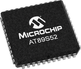
The AT89S52 is a low-power, high-performance CMOS 8-bit microcontroller with 8K in-system programmable Flash memory. It is manufactured using Atmel's high density nonvolatile memory technology and is fully compatible with industry standard 80C51 product instructions and pins. On-chip Flash allows program memory to be system-programmable, which is suitable for conventional programmers. On a single chip, with a clever 8-bit CPU and in-system programmable Flash, the AT89S52 offers a highly flexible and highly effective solution for a wide range of embedded control applications. The AT89S52 microcontroller provides some of the standard features: 8K bytes of Flash, 256 bytes of RAM, 32 bits of I / O lines, watchdog timer, two data pointers, three 16-bit timer / counters, Interrupt structure, full duplex serial port, on-chip crystal oscillator and clock circuit. In addition, AT89S52 microcontroller design and operating frequency can be reduced to 0 HZ static logic, supports two kinds of software selectable power-saving mode. In Idle mode, the CPU stops working while the RAM, timer / counter, serial port, external interrupt system can continue to work. In power-down protection mode, the RAM contents can be saved, but the oscillator will be frozen and the microcontroller will stop working until the next interrupt or hardware reset. The pin configuration shown in the figure: (three packages: PDIP, PLCC, TQFP)
Pin Description:
Port 0: Port 0 is an 8-bit open-drain bi-directional I / O port. As output, each bit can drive 8 TTL logic levels. When writing "1" to port P0, the pin functions as a high-impedance input. Port 0 is also used as the lower 8 bits of address / data when accessing external programs and data memory. In this mode, P0 has an internal pull-up resistor. Port P0 is also used to receive instruction bytes during flash programming. Instruction bytes are output during program verification. Program verification, the need for external pull-up resistor.
Port 1: Port 1 is an 8-bit bidirectional I / O port with an internal pull-up resistor. The p1 output buffer drives 4 TTL logic levels. When writing "1" to port P1, the internal pull-up resistor pulls the port high to be used as the input port. When used as an input, the pin that is pulled low externally will output current (IIL) due to internal resistance. In addition, P1.0 and P1.2 provide the external count input (P1.0 / T2) of timer / counter 2 and the trigger input (P1.1 / T2EX) of timer / counter 2, respectively, as shown in the following table. Port 1 receives the lower 8-bit address byte during flash programming and verification.
Port 2: Port 2 is an 8-bit bidirectional I / O port with internal pull-ups. The P2 output buffer drives 4 TTL logic levels. When "1" is written to port P2, the internal pull-up resistor pulls the port high to be used as the input port. When used as an input, the pin that is pulled low externally will output current (IIL) due to internal resistance. When accessing external program memory or reading external data memory with a 16-bit address (eg, executing MOVX @DPTR), port 2 sends out a high eight-bit address. Port 2 uses a strong internal pull-up for this application. Port P2 outputs the contents of the P2 latch when accessing external data memory using an 8-bit address such as MOVX @ RI. In flash programming and verification, P2 port also receives the upper 8-bit address bytes and some control signals.
Port 3: Port 3 is an 8-bit bidirectional I / O port with an internal pull-up resistor. The p3 output buffer drives 4 TTL logic levels. When writing "1" to port P3, the internal pull-up resistor pulls the port high and can be used as an input port at this time. When used as an input, the pin that is pulled low externally will output current (IIL) due to internal resistance. Port 3 is also used as AT89S52 special function (second function). During flash programming and calibration, port 3 also receives some control signals.
In addition, Port 3 also receives some FLASH flash programming and program control of the control signal.
RST - reset input. When the oscillator is in operation, a RST pin high above two machine cycles will be a microcontroller reset.
ALE / PROG - The ALE (Address Latch Enable) output pulse is used to latch the lower 8 bytes of an address when accessing external program memory or data memory. In general, ALE still outputs a fixed pulse signal at 1/6 of the oscillation frequency of the clock, so it can output the clock externally or for timing purposes. Note that one ALE pulse is skipped every time an external data memory is accessed. This pin is also used to enter a programming pulse (PROG) during programming of FLASH memory. If necessary, ALE operation can be disabled by setting the D0 bit of the 8EH unit in the special function register (SFR) area. After this bit is set, only one MOVX and MOVC instruction can activate ALE. In addition, the pin will be slightly pulled up, the implementation of an external program microcontroller, you should set the ALE disable bit is invalid.
PSEN - Program Memory Enable (PSEN) The output is the read strobe for external program memory. When the AT89C52 is fetched (or data) from the external program memory, PSEN is valid twice per machine cycle, that is, two pulses are output at During this period, the PSEN signal will be skipped twice when accessing the external data memory.
EA / VPP - External Access Enable To enable the CPU to access only external program memory (address 0000H-FFFFH), the EA pin must be held low (ground). It should be noted that if the encryption bit LB1 is programmed, the state of EA end will be latched internally during reset. If EA terminal is high level (then Vcc terminal), CPU executes internal program memory instruction. When FLASH memory is programmed, this pin plus + 12V programming allows power supply Vpp, of course, this must be the device is using 12V programming voltage Vpp.
More electronic tutorials:
ElectronicsTeacher.com : Electronic Tutorials, Electronic Project Kits, Robotics Guide for Students, Amateur and Professionals. Computer Architecture and Digital Circuits.
 Author:Brittany Antonia (The author of article owns the copyright.)





