
-
Products
-
Featured Products
-
IT infrastructure
- Hard Drives
- OEM Souring
- CPU
- IT infrastructure Memory
- Spare Parts
- Cables
- Power Supply Units
- Adapters
- Controllers
- Server
- Switch
- Network Cards
- IT infrastructure Accessories
- Storage Machines
- Systemboard
- Sfp
- Harddrives
- Heatsink
- Fan
- Rack Options
- Licenses
- Battery
- IT Racks
- Graphics
- Io Expansions
- Routers
- San
- Access Point
- Blades
- Firewalls
- Expansion Cards
- Software
- Chassis
- Flex System
- Ups
- Wifi Controller
- Bladecenters
- Rack Mounts
- Monitors
- Antenna
- Phones
- Hmc
- HOT - SALES and EOL Components
- Hard To Find
- END - OF - LIFE
- Electronic Wholesale
- 88E series
- Maxim Series
- TPS series
- STM series
- SEE ALL

-
IT infrastructure
-
Integrated Circuits (ICs)
- Integrated Circuits (ICs) Kits
- Specialized ICs
- Memory
- Audio Special Purpose
- Clock/Timing
- Data Acquisition
-
Embedded
- Embedded - CPLDs (Complex Programmable Logic Devices)
- Embedded - DSP (Digital Signal Processors)
- Embedded - FPGAs (Field Programmable Gate Array)
- Embedded - Microcontrollers
- Embedded - Microcontrollers - Application Specific
- Embedded - Microprocessors
- Embedded - PLDs (Programmable Logic Device)
- Embedded - System On Chip (SoC)
- SEE ALL
-
Interface
- Interface - Analog Switches - Special Purpose
- Interface - Analog Switches, Multiplexers, Demultiplexers
- Interface - CODECs
- Interface - Controllers
- Interface - Drivers, Receivers, Transceivers
- Interface - Encoders, Decoders, Converters
- Interface - Filters - Active
- Interface - I/O Expanders
- Interface - Modems - ICs and Modules
- Interface - Sensor and Detector Interfaces
- Interface - Serializers, Deserializers
- Interface - Signal Buffers, Repeaters, Splitters
- Interface - Signal Terminators
- Interface - Specialized
- Interface - Telecom
- Interface - UARTs (Universal Asynchronous Receiver Transmitter)
- Interface - Voice Record and Playback
- Interface - Sensor, Capacitive Touch
- SEE ALL
- Linear
-
Logic
- Logic - Buffers, Drivers, Receivers, Transceivers
- Logic - Comparators
- Logic - Counters, Dividers
- Logic - FIFOs Memory
- Logic - Flip Flops
- Logic - Gates and Inverters
- Logic - Latches
- Logic - Multivibrators
- Logic - Parity Generators and Checkers
- Logic - Shift Registers
- Logic - Signal Switches, Multiplexers, Decoders
- Logic - Specialty Logic
- Logic - Translators, Level Shifters
- Logic - Universal Bus Functions
- Logic - Gates and Inverters - Multi - Function, Configurable
-
PMIC
- PMIC - Power Over Ethernet (PoE) Controllers
- PMIC - Power Supply Controllers, Monitors
- PMIC - RMS to DC Converters
- PMIC - Supervisors
- PMIC - Thermal Management
- PMIC - V/F and F/V Converters
- PMIC - Voltage Reference
- PMIC - Voltage Regulators - DC DC Switching Controllers
- PMIC - Voltage Regulators - DC DC Switching Regulators
- PMIC - Voltage Regulators - Linear
- PMIC - Voltage Regulators - Linear Regulator Controllers
- PMIC - Voltage Regulators - Linear + Switching
- PMIC - Voltage Regulators - Special Purpose
- PMIC - AC DC Converters, Offline Switchers
- PMIC - Battery Chargers
- PMIC - Battery Management
- PMIC - Current Regulation/Management
- PMIC - Display Drivers
- PMIC - Energy Metering
- PMIC - Full, Half - Bridge Drivers
- PMIC - Gate Drivers
- PMIC - Hot Swap Controllers
- PMIC - Laser Drivers
- PMIC - LED Drivers
- PMIC - Lighting, Ballast Controllers
- PMIC - Motor Drivers, Controllers
- PMIC - OR Controllers, Ideal Diodes
- PMIC - PFC (Power Factor Correction)
- PMIC - Power Distribution Switches, Load Drivers
- PMIC - Power Management - Specialized
- PMIC - Voltage Regulators - Linear, Low Drop Out (LDO) Regulators
- SEE ALL
- SEE ALL
-
Discrete Semiconductor Products
- Current Regulation - Diodes, Transistors
- IGBTs - Arrays
- Thyristors—SCRs
- Bridge Rectifiers
- Diacs, Sidacs
- Diodes - Zener - Arrays
- Diodes - Zener - Single
- Diodes, Rectifiers - Arrays
- Diodes, Rectifiers - Single
- FETs - Arrays
- FETs - Single
- IGBTs - Modules
- IGBTs - Single
- JFETs (Junction Field Effect)
- Power Drivers - Modules
- RFFETs
- SCRs - Single - Modules
- SCRs - Single
- Triacs
- Variable Capacitance Diodes (Varicaps, Varactors)
- RF Diodes
-
TRANSISTORS
- Transistors – FETs, MOSFETs – Single
- Transistors - FETs, MOSFETs Arrays
- RF Transistors (BJT)
- Transistors - FETs, MOSFETs - RF
- Transistors - Special Purpose
- Transistors (BJT) - Arrays
- Transistors (BJT) - Arrays, Pre - Biased
- Transistors (BJT) - Single
- Transistors (BJT) - Single, Pre - Biased
- Darlington Transistor
- SEE ALL
- SEE ALL
- Memory Cards, Modules
-
Sensors, Transducers
- Sensor Interface Junction Blocks
- Sensors, Transducers -Magnets Sensor -Matched Magnets
- Sensors, Transducers -Position Sensors- Angle, Linear Position Measuring
- Sensor Cable Assemblies
- Capacitive Touch Sensors, Proximity Sensor ICs
- Current Transducers
- Encoders
- Image Sensors, Camera
- IrDA Transceiver Modules
- Moisture Sensors, Humidity
- Position Sensors - Angle, Linear Position Measuring
- Pressure Sensors, Transducers
- Proximity Sensors
-
Optical Sensors
- Optical Sensors - Ambient Light, IR, UV Sensors
- Optical Sensors - Photo Detectors - Remote Receiver
- Optical Sensors - Photodiodes
- Optical Sensors - Photointerrupters - Slot Type - Logic Output
- Optical Sensors - Photointerrupters - Slot Type - Transistor Output
- Optical Sensors - Phototransistors
- Optical Sensors - Reflective - Analog Output
- Optical Sensors - Image Sensors, Camera
- SEE ALL
- Motion Sensors
- Temperature Sensors
- Magnetic Sensors
- Proximity Sensors - Industrial
- SEE ALL
-
Optoelectronics
- Fiber Optic Transceiver Modules
- Display Bezels, Lenses
- Display Backlights
- LED Emitters - Infrared, UV, Visible
- Ballasts, Inverters
- Optocouplers/Photocouplers
- Infrared, UV, Visible Emitters
- LED Indication - Discrete
- LEDs - Circuit Board Indicators, Arrays, Light Bars, Bar Graphs
- Optics - LEDs - Light Pipes
- Panel Indicators, Pilot Lights
- LEDs - Spacers, Standoffs
- Fiber Optics
- Led Lighting
- Display Modules
- LCD, OLED, Graphic
- LED Character and Numeric
- Custom Products
- SEE ALL
- Circuit Protection
-
Connectors, Interconnects
- AC Power Connectors
- Keystone Connector Accessories
- Card Edge Connector Housings
- Card Edge Connector Contacts
- Headers & Wire Housings
- LGH Connectors
- Terminals—Screw Connectors
- USB, DVI, HDMI Connectors —USB, DVI, HDMI Connector Assemblies
- Industrial Controls, Meters——Controllers——Specialty Controllers
- Card Edge Connectors - Edgeboard Connectors
- Circular Connectors
- Memory Connectors - PC Card Sockets
- Modular Connectors
- Pluggable Connectors
- Power Entry Connectors - Inlets, Outlets, Modules
- Rectangular - Board to Board Connectors
- Rectangular Connectors
- Sockets for ICs, Transistors
- Terminal Blocks
- Terminals
- USB, DVI, HDMI Connectors
- Backplane Connectors
- Coaxial Connectors (RF)
- FFC, FPC (FlatFlexible) Connectors
- D - SUB, D - SHAPED connectors
- Terminals - PC Pin Receptacles, Socket Connectors
- Terminals - PC Pin, Single Post Connectors
- Terminals - Quick Connects, Quick Disconnect Connectors
- Terminals - Specialized Connectors
- Terminals - Wire Splice Connectors
- Terminals - Wire to Board Connectors
- FFC, FPC (FlatFlexible) Connector Assemblies
- Heavy Duty Connector Frames
- Heavy Duty Connector Accessories
- Heavy Duty Connector Inserts, Modules
- Modular Connector Jacks
- Modular Connector Jacks With Magnetics
- Modular/Ethernet Connector (RJ45, RJ11) Jacks
- Pluggable Connector Assemblies
- Rectangular - Board to Board Connectors - Arrays, Edge Type, Mezzanine
- Rectangular Connectors - Board In, Direct Wire to Board
- Rectangular Connectors - Free Hanging, Panel Mount
- Rectangular Connectors - Headers, Male Pins
- Rectangular Connectors - Headers, Receptacles, Female Sockets
- Rectangular Connector - Accessories
- Rectangular Connector Contacts
- Rectangular Connector Housings
- Rectangular Connector - Spring Loaded
- Solid State Lighting Connector - Assemblies
- SEE ALL
- Capacitors
- Resistors
- Relays
- Isolators
- Filters
- Power Supplies - Board Mount
-
RF/IF and RFID
- RFID Reader Modules
- RF and Wireless >RF Power Dividers/Splitters
- Attenuators
- Balun
- RF Amplifiers
- RF Antennas
- RF Demodulators
- RF Detectors
- RF Diplexers
- RF Directional Coupler
- RF Evaluation and Development Kits, Boards
- RF Front End (LNA + PA)
- RF Misc ICs and Modules
- RF Mixers
- RF Modulators
- RF Power Dividers/Splitters
- RF Receivers
- RF Switches
- RF Transceiver ICs
- RF Transceiver Modules
- RF Transmitters
- RFID, RF Access, Monitoring ICs
- RF Multiplexers
- SEE ALL
- Crystals, Oscillators and Resonators
-
Uncategorized
- Audio Products
- Cable Assemblies
- Cables, Wires
- Cables, Wires - Management
- Hardware, Fasteners, Accessories
- Inductors, Coils, Chokes
- Industrial Controls, Meters
- Potentiometers, Variable Resistors
-
Programmers, Development Systems
- Evaluation Boards - Embedded - Complex Logic (FPGA, CPLD)
- Evaluation Boards
- Evaluation Boards—RF Evaluation and Development Kits, Boards
- Evaluation and Demonstration Boards and Kits
- Evaluation Boards - Analog to Digital Converters (ADCs)
- Evaluation Boards - Audio Amplifiers
- Evaluation Boards - DC/DC & AC/DC (Off - Line)SMPS
- Evaluation Boards - Embedded - MCU, DSP
- Evaluation Boards - Expansion Boards
- Evaluation Boards - Op Amps
- Evaluation Boards - Sensors
- Evaluation Boards - Linear Voltage Regulators
- Evaluation Boards - RF, RFID, Wireless
- SEE ALL
- Switches
- Transformers
- Tools and Supplies
- Prototyping, Fabrication Products
- SEE ALL
-
Featured Products
-
Manufacturers
- Altera
- Analog Devices Inc.
- Atmel
- Bosch Sensortec
- Cypress Semiconductor Corp
- Diodes Incorporated
- Freescale Semiconductor - NXP
- FTDI, Future Technology Devices International Ltd
- Infineon Technologies
- Linear Technology
- Maxim Integrated
- Microchip Technology
- Micron Technology Inc.
- NXP / Nexperia
- ON Semiconductor
- Silicon Labs
- STMicroelectronics
- Texas Instruments
- Allegro MicroSystems, LLC
- Vishay
- SEE ALL
- My Account
- Supports
- About Us
- Group
- Contact Us
Four Important skills for Quickly and Efficientyl Wiring PCB
In the PCB design process, The method of wiring is full of challenges, engineers in this process are often faced with various problems. This article will be the first to do a simple explanation about PCB,based on the principle of wiring at the same time , and finally will bring four practical PCB wiring skills to you.
Here are some good wiring tips and tricks:
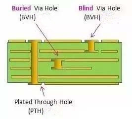
First of all, to do a basic introduction, PCB layers can be divided into single, double and multi-layer, the single layer is now basically eliminated.The Double plate is now in general used in the sound system , multi-layer refers to the 4-layer and 4 layers of the board,and in general, the density of the components for the general requirements of the 4-layer will be enough. From the perspective of the hole can be divided into through-hole, blind hole, and buried hole. Through hole is a hole from the top layer directly to the bottom; blind hole from the top or bottom hole to the middle layer, and then do not continue to wear, and the advantage is that the location of this hole is not from the plug to the tail, Other layers in the location of this hole can still be traced; buried through the hole is the middle layer to the middle layer, the surface is completely invisible. The details are shown below.
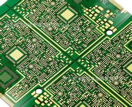
Pcb board
Before the automatic routing, you should use interactive lines in advance, input and output side of the line should not be adjacent to parallel to avoid reflection interference. If necessary, ground isolation can be added , and the adjacent layers of the wiring should be perpendicular to each other,because of the parallel relatively easy to produce parasitic coupling. The wiring rate of the automatic routing depends on a good layout. The wiring rules can be preset, such as the number of alignment curves, the number of vias, the number of steps, and so on. In General,the first things is to explore the wirings, fastly connect short-term, and then through the labyrinth of wiring, optimize the whole routing path, it can be disconnected according to the needs of the line and try to re-wiring to improve overall cabling effect.
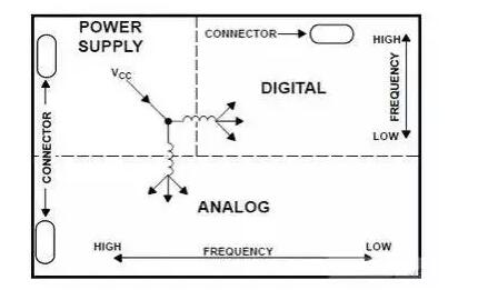
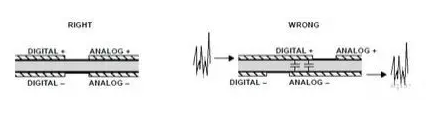
For the layout, the principle is to separate the digital and analog as far as possible, other principle is to keep the distance between low-speed and high-speed close. The most basic principle is to separate the digital ground and analog ground, digital ground are all switching devices, the current moment in the switch are great, so the digital ground and analog ground can not be mixed together. A recommended layout can look like the following figure.
Pcb wiring
1, Attentions between the power supply and ground wiring
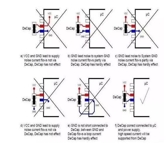
- Add the decoupling capacitor betweenpower supply and ground wires. Be sure that power supply will be through the decoupling capacitor first,and then connected to the pin .The following figure lists a few wrong connection method and a correct connection method.Have you made such mistakes? Decoupling capacitors generally have two roles, one is to provide the chip instantaneous high current, the second is to remove the power supply noise, on the one hand is to make the power of the noise as little as possible impact on the chip, the other is the chip noise do not affect power supply.
Wiring considerations between the power supply and ground
(2) try to widen the power supply and ground, the relationship is: ground >power line>signal line.
- can use a large area of copper layer for the ground
2, The treatment when digital circuits and analog circuits be mixed
Now, many of the PCB no longer has a single function of the circuit, but by mixing the digital circuit and analog circuit , so we need to pay attention to the mutual interference between them, especially ground noise interference.
As the high-frequency of digital circuit and high-sensitive analog circuit,to the signal line, the high-frequency signal lines should be set as far as possible away from the sensitive analog circuit devices, but for the entire PCB, PCB ground on the outside of the node may only one, it must be dealt with in the PCB internal digital circuit and analog circuit common ground problems, and in the circuit board, the digital circuit ground and analog circuit ground is actually separate, but in the PCB and the outside world connection Of the interface (such as plugs, etc.). The ground of the digital circuit is slightly shorted to the analog circuit. Note that there is only one connection point and there is no common ground on the PCB. This is determined by the system design.
3, Solution of the corner line
Usually, there will be changes in the thickness of the corner of the line, but the thickness of the diameter may change . Corner method For the line thickness changes, the right angle is the worst, 45-degree angle is better, rounded corner is the best. But the rounded corner of the PCB design is more trouble in terms of treatment, it is generally decided by the degree of sensitivity.it will be o to use a 45-degree angle , only those very sensitive lines need to use fillet.
For the processing of the corner of the line
4, After the design ,you should check the design rules
No matter what to do, work should be checked after the completion, So that we can be surer that we draw out of the circuit board is a qualified product. Our general inspection has the following aspects:
(1) Whether the distance between the wire and the wire, the wire and the component pad, the wire and the through hole, the component pad and the through hole, the through hole and the through hole is reasonable, whether meets the production request.
The width of the groundand the power cord is appropriate.
(3) If you take the best measures to the signal line, such as the length of the shortest, plus protection lines, input lines and output lines are clearly separated.
(4) Imitate circuits and digital circuits, whether there is a separate ground.
(5) If the icon, marking will cause a signal short-circuit.
(6) To modify some of the line which is not ideal.
(7) Whether the PCB on the process line, resistance welding production process is consistent with the requirements, solder size is appropriate.
In short, the above skills and methods are the experience of the discussion, it is worth when drawing PCB board.In the process of drawing PCB map ,we need to professionally use mapping tools, but also have a solid theoretical knowledge and rich practical Experience, which can help you quickly and efficiently complete your PCB map. But there is one very important, that is, we must be careful, whether it is wiring or the overall layout of each step must be very careful and serious.if you make a small mistake ,it may lead to your final product become waste.we prefer to spend more time in the drawing process to carefully check the details of the part ,rather than go back to check the problem.
 Author :Darcy Beaufort — WIN SOURCE ELECTRONICS





