
-
Products
-
Featured Products
-
IT infrastructure
- Hard Drives
- OEM Souring
- CPU
- IT infrastructure Memory
- Spare Parts
- Cables
- Power Supply Units
- Adapters
- Controllers
- Server
- Switch
- Network Cards
- IT infrastructure Accessories
- Storage Machines
- Systemboard
- Sfp
- Harddrives
- Heatsink
- Fan
- Rack Options
- Licenses
- Battery
- IT Racks
- Graphics
- Io Expansions
- Routers
- San
- Access Point
- Blades
- Firewalls
- Expansion Cards
- Software
- Chassis
- Flex System
- Ups
- Wifi Controller
- Bladecenters
- Rack Mounts
- Monitors
- Antenna
- Phones
- Hmc
- Hard To Find
- END - OF - LIFE
- Electronic Wholesale
- 88E series
- Maxim Series
- TPS series
- STM series
- HOT - SALES and EOL Components
- SEE ALL

-
IT infrastructure
-
Integrated Circuits (ICs)
- Integrated Circuits (ICs) Kits
- Clock/Timing
- Data Acquisition
-
Embedded
- Embedded - CPLDs (Complex Programmable Logic Devices)
- Embedded - DSP (Digital Signal Processors)
- Embedded - FPGAs (Field Programmable Gate Array)
- Embedded - Microcontrollers
- Embedded - Microcontrollers - Application Specific
- Embedded - Microprocessors
- Embedded - PLDs (Programmable Logic Device)
- Embedded - System On Chip (SoC)
- SEE ALL
-
Interface
- Interface - Analog Switches - Special Purpose
- Interface - Analog Switches, Multiplexers, Demultiplexers
- Interface - CODECs
- Interface - Controllers
- Interface - Drivers, Receivers, Transceivers
- Interface - Encoders, Decoders, Converters
- Interface - Filters - Active
- Interface - I/O Expanders
- Interface - Modems - ICs and Modules
- Interface - Sensor and Detector Interfaces
- Interface - Serializers, Deserializers
- Interface - Signal Buffers, Repeaters, Splitters
- Interface - Signal Terminators
- Interface - Specialized
- Interface - Telecom
- Interface - UARTs (Universal Asynchronous Receiver Transmitter)
- Interface - Voice Record and Playback
- Interface - Sensor, Capacitive Touch
- SEE ALL
- Linear
-
Logic
- Logic - Gates and Inverters - Multi - Function, Configurable
- Logic - Buffers, Drivers, Receivers, Transceivers
- Logic - Comparators
- Logic - Counters, Dividers
- Logic - FIFOs Memory
- Logic - Flip Flops
- Logic - Gates and Inverters
- Logic - Latches
- Logic - Multivibrators
- Logic - Parity Generators and Checkers
- Logic - Shift Registers
- Logic - Signal Switches, Multiplexers, Decoders
- Logic - Specialty Logic
- Logic - Translators, Level Shifters
- Logic - Universal Bus Functions
-
PMIC
- PMIC - Power Over Ethernet (PoE) Controllers
- PMIC - Power Supply Controllers, Monitors
- PMIC - RMS to DC Converters
- PMIC - Supervisors
- PMIC - Thermal Management
- PMIC - V/F and F/V Converters
- PMIC - Voltage Reference
- PMIC - Voltage Regulators - DC DC Switching Controllers
- PMIC - Voltage Regulators - DC DC Switching Regulators
- PMIC - Voltage Regulators - Linear
- PMIC - Voltage Regulators - Linear Regulator Controllers
- PMIC - Voltage Regulators - Linear + Switching
- PMIC - Voltage Regulators - Special Purpose
- PMIC - AC DC Converters, Offline Switchers
- PMIC - Battery Chargers
- PMIC - Battery Management
- PMIC - Current Regulation/Management
- PMIC - Display Drivers
- PMIC - Energy Metering
- PMIC - Full, Half - Bridge Drivers
- PMIC - Gate Drivers
- PMIC - Hot Swap Controllers
- PMIC - Laser Drivers
- PMIC - LED Drivers
- PMIC - Lighting, Ballast Controllers
- PMIC - Motor Drivers, Controllers
- PMIC - OR Controllers, Ideal Diodes
- PMIC - PFC (Power Factor Correction)
- PMIC - Power Distribution Switches, Load Drivers
- PMIC - Power Management - Specialized
- PMIC - Voltage Regulators - Linear, Low Drop Out (LDO) Regulators
- SEE ALL
- Specialized ICs
- Memory
- Audio Special Purpose
- SEE ALL
-
Discrete Semiconductor Products
- Current Regulation - Diodes, Transistors
- IGBTs - Arrays
- Thyristors—SCRs
-
TRANSISTORS
- Transistors – FETs, MOSFETs – Single
- Transistors - FETs, MOSFETs Arrays
- RF Transistors (BJT)
- Transistors - FETs, MOSFETs - RF
- Transistors - Special Purpose
- Transistors (BJT) - Arrays
- Transistors (BJT) - Arrays, Pre - Biased
- Transistors (BJT) - Single
- Transistors (BJT) - Single, Pre - Biased
- Darlington Transistor
- SEE ALL
- Bridge Rectifiers
- Diacs, Sidacs
- Diodes - Zener - Arrays
- Diodes - Zener - Single
- Diodes, Rectifiers - Arrays
- Diodes, Rectifiers - Single
- FETs - Arrays
- FETs - Single
- IGBTs - Modules
- IGBTs - Single
- JFETs (Junction Field Effect)
- Power Drivers - Modules
- RFFETs
- SCRs - Single - Modules
- SCRs - Single
- Triacs
- Variable Capacitance Diodes (Varicaps, Varactors)
- RF Diodes
- SEE ALL
- Memory Cards, Modules
-
Sensors, Transducers
- Sensor Interface Junction Blocks
- Sensors, Transducers -Magnets Sensor -Matched Magnets
- Sensors, Transducers -Position Sensors- Angle, Linear Position Measuring
- Sensor Cable Assemblies
-
Optical Sensors
- Optical Sensors - Ambient Light, IR, UV Sensors
- Optical Sensors - Photo Detectors - Remote Receiver
- Optical Sensors - Photodiodes
- Optical Sensors - Photointerrupters - Slot Type - Logic Output
- Optical Sensors - Photointerrupters - Slot Type - Transistor Output
- Optical Sensors - Phototransistors
- Optical Sensors - Reflective - Analog Output
- Optical Sensors - Image Sensors, Camera
- SEE ALL
- Motion Sensors
- Temperature Sensors
- Magnetic Sensors
- Capacitive Touch Sensors, Proximity Sensor ICs
- Current Transducers
- Encoders
- Image Sensors, Camera
- IrDA Transceiver Modules
- Moisture Sensors, Humidity
- Position Sensors - Angle, Linear Position Measuring
- Pressure Sensors, Transducers
- Proximity Sensors
- Proximity Sensors - Industrial
- SEE ALL
-
Optoelectronics
- Fiber Optic Transceiver Modules
- Display Bezels, Lenses
- Display Backlights
- LED Emitters - Infrared, UV, Visible
- Ballasts, Inverters
- Optocouplers/Photocouplers
- LEDs - Spacers, Standoffs
- Fiber Optics
- Led Lighting
- Display Modules
- Infrared, UV, Visible Emitters
- LED Indication - Discrete
- LEDs - Circuit Board Indicators, Arrays, Light Bars, Bar Graphs
- Optics - LEDs - Light Pipes
- Panel Indicators, Pilot Lights
- LCD, OLED, Graphic
- LED Character and Numeric
- Custom Products
- SEE ALL
- Circuit Protection
-
Connectors, Interconnects
- AC Power Connectors
- Keystone Connector Accessories
- Card Edge Connector Housings
- Card Edge Connector Contacts
- Headers & Wire Housings
- LGH Connectors
- Terminals—Screw Connectors
- USB, DVI, HDMI Connectors —USB, DVI, HDMI Connector Assemblies
- Industrial Controls, Meters——Controllers——Specialty Controllers
- D - SUB, D - SHAPED connectors
- Card Edge Connectors - Edgeboard Connectors
- Circular Connectors
- Memory Connectors - PC Card Sockets
- Modular Connectors
- Pluggable Connectors
- Power Entry Connectors - Inlets, Outlets, Modules
- Rectangular - Board to Board Connectors
- Rectangular Connectors
- Sockets for ICs, Transistors
- Terminal Blocks
- Terminals
- USB, DVI, HDMI Connectors
- Backplane Connectors
- Coaxial Connectors (RF)
- FFC, FPC (FlatFlexible) Connectors
- Terminals - PC Pin Receptacles, Socket Connectors
- Terminals - PC Pin, Single Post Connectors
- Terminals - Quick Connects, Quick Disconnect Connectors
- Terminals - Specialized Connectors
- Terminals - Wire Splice Connectors
- Terminals - Wire to Board Connectors
- FFC, FPC (FlatFlexible) Connector Assemblies
- Heavy Duty Connector Frames
- Heavy Duty Connector Accessories
- Heavy Duty Connector Inserts, Modules
- Modular Connector Jacks
- Modular Connector Jacks With Magnetics
- Modular/Ethernet Connector (RJ45, RJ11) Jacks
- Pluggable Connector Assemblies
- Rectangular - Board to Board Connectors - Arrays, Edge Type, Mezzanine
- Rectangular Connectors - Board In, Direct Wire to Board
- Rectangular Connectors - Free Hanging, Panel Mount
- Rectangular Connectors - Headers, Male Pins
- Rectangular Connectors - Headers, Receptacles, Female Sockets
- Rectangular Connector - Accessories
- Rectangular Connector Contacts
- Rectangular Connector Housings
- Rectangular Connector - Spring Loaded
- Solid State Lighting Connector - Assemblies
- SEE ALL
- Capacitors
- Resistors
- Relays
- Isolators
- Filters
- Power Supplies - Board Mount
-
RF/IF and RFID
- RFID Reader Modules
- RF and Wireless >RF Power Dividers/Splitters
- RF Multiplexers
- Attenuators
- Balun
- RF Amplifiers
- RF Antennas
- RF Demodulators
- RF Detectors
- RF Diplexers
- RF Directional Coupler
- RF Evaluation and Development Kits, Boards
- RF Front End (LNA + PA)
- RF Misc ICs and Modules
- RF Mixers
- RF Modulators
- RF Power Dividers/Splitters
- RF Receivers
- RF Switches
- RF Transceiver ICs
- RF Transceiver Modules
- RF Transmitters
- RFID, RF Access, Monitoring ICs
- SEE ALL
- Crystals, Oscillators and Resonators
-
Uncategorized
- Audio Products
- Cable Assemblies
- Cables, Wires
- Cables, Wires - Management
- Hardware, Fasteners, Accessories
- Inductors, Coils, Chokes
- Industrial Controls, Meters
- Potentiometers, Variable Resistors
-
Programmers, Development Systems
- Evaluation Boards - Embedded - Complex Logic (FPGA, CPLD)
- Evaluation Boards
- Evaluation Boards—RF Evaluation and Development Kits, Boards
- Evaluation Boards - Linear Voltage Regulators
- Evaluation and Demonstration Boards and Kits
- Evaluation Boards - Analog to Digital Converters (ADCs)
- Evaluation Boards - Audio Amplifiers
- Evaluation Boards - DC/DC & AC/DC (Off - Line)SMPS
- Evaluation Boards - Embedded - MCU, DSP
- Evaluation Boards - Expansion Boards
- Evaluation Boards - Op Amps
- Evaluation Boards - Sensors
- Evaluation Boards - RF, RFID, Wireless
- SEE ALL
- Switches
- Transformers
- Tools and Supplies
- Prototyping, Fabrication Products
- SEE ALL
-
Featured Products
-
Manufacturers
- Altera
- Analog Devices Inc.
- Atmel
- Bosch Sensortec
- Cypress Semiconductor Corp
- Diodes Incorporated
- Freescale Semiconductor - NXP
- FTDI, Future Technology Devices International Ltd
- Infineon Technologies
- Linear Technology
- Maxim Integrated
- Microchip Technology
- Micron Technology Inc.
- NXP / Nexperia
- ON Semiconductor
- Silicon Labs
- STMicroelectronics
- Texas Instruments
- Allegro MicroSystems, LLC
- Vishay
- SEE ALL
- My Account
- Supports
- About Us
- Group
- Contact Us
What is ADC0809?
ADC0809 is a CMOS process 8-channel, 8-bit successive approximation A / D converter manufactured by National Semiconductor. It has an internal 8-channel multiplexer that can latch the decoded signal based on the address code and only gate one of the eight analog input signals for A / D conversion. Is currently the most widely used 8 general-purpose A / D chip.
1.ADC0809 the main features
1) 8 input channels, 8-bit A / D converter, the resolution is 8 bits.
2) has a conversion start and stop control.
3) Conversion time is 100μs (clock is 640kHz), 130μs (clock is 500kHz)
4) Single +5 V power supply
5) Analog input voltage range 0 ~ + 5V, without zero and full scale calibration.
6) Operating temperature range of -40 ~ +85 degrees Celsius 7) Low power consumption, about 15mW.
2.ADC0809's internal structure
ADC0809 is a CMOS monolithic successive approximation A / D converter, the internal structure shown in Figure 13.22, which consists of 8 analog switches, address latch and decoder, comparator, 8-bit switch tree A / D converter Device, successive approximation register, logic control and timing circuit.
3.ADC0809's external features (pin function)
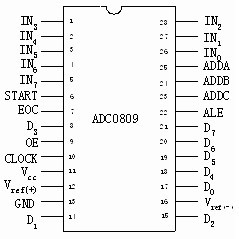
ADC0809 chip has 28 pins, dual in-line package, as shown in Figure 13.23. The following describes each pin function.
IN0 ~ IN7: 8 analog inputs.
2-1 ~ 2-8: 8-bit digital output.
ADDA, ADDB, ADDC: 3-bit address input lines for gating one of the 8 analog inputs
ALE: Address latch enable signal, input, active high.
START: A / D conversion start pulse input, enter a positive pulse (at least 100ns wide) to start (pulse rising edge 0809 reset, falling edge start A / D conversion).
EOC: A / D conversion end signal, output, when the A / D conversion is completed, this terminal outputs a high level (during the conversion has been low).
OE: Data output enable signal, input, active high. When the A / D conversion is finished, this end input a high level, in order to open the output tri-state gate, the output digital.
CLK: clock input. Requirements clock frequency is not higher than 640KHZ.
REF (+), REF (-): Reference voltage.
Vcc: power supply, single + 5V.
GND: ground.
 Author:Brittany Antonia (The author of article owns the copyright.)





